Lithography Machine Basic and Development
Posted by Chandler Buff on June 14th, 2023
Overview
The semiconductor industry has followed Moore's Law for more than half a century, driving a series of technique innovations. As the electronic device size is getting closer and closer to the physical limit, whether Moore's Law is still effective for the development of new generation process nodes has become a question. Among them, lithography is the frontier to verify Moore's Law.
Optical Wavelength Development
Since the first planar IC appeared in 1958, lithography technology has made great contributions to microelectronics technology development. In the semiconductors manufacturing, it is necessary to transfer the circuit pattern to the single crystal surface or the dielectric layer through lithography tech. So its continuous breakthrough has promoted the density and performance of integrated circuits greatly, and reduced cost.
In the past 60 years, lithography technology has broken through the resolution limit again and again, and made the IC process limit constantly broken, so Moore's Law is constantly extending. Looking back at the development history, with the continuous shrinking of process nodes, lithography technique has mainly included ultraviolet lithography (UV), deep ultraviolet lithography (DUV) and extreme ultraviolet lithography (EUV). And the wavelength of light also shortens from 436nm, 365nm, 248nm to 193nm, 13.5nm and so on.
Since the 1980s, the wavelength of light used in lithography has changed:
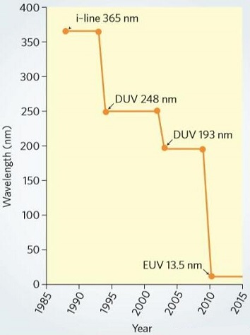
Fig 1: Light Wavelength Change from ASML
Lithography Battle over Chip Giants
Looking back at the development process, the lithography light source was stuck at 193nm and could not progress for 20 years. What happened during this period? Time goes back to the 1960s, there were still more than 20 years before the establishment of ASML, but the integrated circuits had been growing in California, U.S greatly. In the entire process of integrated circuit manufacturing, lithography is the most critical technique. In a word, the principle of a lithography machine is actually as simple as a slide projector, which is to project light through a mask with a circuit diagram onto a wafer coated with photosensitive adhesive. In the early 1960s, the mask plate was attached to the wafer at a size of 1:1, and the wafer was only 1-inch.
For lithography technology, companies such as GCA and Perkin-Elmer started the initial technology and market accumulation. When Philips in the Dutch finally started to develop a lithography machine, GCA has developed a re-exposure machine and put it on the market. As the size of IC gradually shrinks, contact lithography is gradually hard to meet the precision requirements, and the industry begins to seek new breakthroughs. In the late 1970s, Perkin-Elmer gained 90% of the lithography market with projection scanning lithography machines, and became the largest equipment supplier in the semiconductor industry. At the same time, GCA also quickly launched the first stepper lithography machine to compete with the Perkin-Elmer.
By the early 1980s, Prekin-Elmer and GCA in the United States dominated the global lithography machine market, and Nikon and Canon in Japan began to show strong development momentum and seize the market from GCA and P&E. However, Philips fell into a state of stagnation. In 1983, it finally agreed to cooperate with ASM. At this time, its lithography machine research and development had reached a bottleneck period. By 1984, Nikon was on an equal footing with GCA, each with 30% of the market share, Ultratech accounted for about 10%, and the remaining companies such as Eaton, P&E, Canon, and Hitachi each had less than 5%. In the same year, ASML, a joint venture between Philips and ASM, was established, but it was not appreciated in its early days.
In competition and technological evolution, in the mid-1980s, the semiconductor market fell into a big decline. As a result, a group of lithography machine manufacturers have met serious financial problems. Among them, ASM withdrew capital from ASML for self-insurance; GCA and Prekin-Elmer were also affected and acquired successively by General Signal and SVG in 1988 and 1990, because of new product stagnation. At that time, ASML was still small, with only about 10% of the market share, and suffered little loss, and could develop new products according to the original plan. However, American companies, which still occupied most of the market in 1980, were completely replaced by Japanese companies by the end of the 1980s.
Lithography Tech Fork
From above mentioned, it can be obtained that changes in the lithography market also correspond to changes in lithography technology. In electronics, Moore's Law has been regarded as the criterion by the integrated circuit industry for a long time. To obey it, it is necessary to reduce the exposure critical dimension (CD) by 30%-50% every two years. This leads to a formula: CD=K1*λ/NA. It can be seen from the formula that the exposure critical dimension is related to the three parameters of wavelength, numerical aperture and process factor. According to the requirements, to reduce the exposure critical dimension, only need to reduce the wavelength λ, increase the numerical aperture NA or reduce the process factor K1.
Among them, shortening the wavelength is a more direct method. From the 1960s to the mid-1980s, contact lithography machines, proximity lithography machines and projection lithography machines mainly used mercury lamp light sources, and their spectral lines were g-line (436nm), h-line (405nm) and i-line (365nm). With the evolution of technology, 248nm KrF lasers have been used in succession. In the 1990s, dry lithography technology has been difficult to maintain the evolution of Moore's Law, and finally stagnated at 193nm DUV lithography technology, which is the famous ArF excimer laser. At this time, the wavelength of the light source of the lithography machine was stuck at 193nm, which became a difficulty facing the whole industry, and also caused problems in the chip manufacturing process at the 65/45nm technology node.
In the second half of the 1990s, everyone was studying the technology to replace the 193nm lithography. In order to "grind" the 193nm light wave finely, most of the semiconductor industry participated and divided into two teams:
Conservatives such as Nikon and Canon advocate the use of 157nm wavelength light sources on the basis of the previous generation technology; the new EUV LLC alliance is betting on the more radical extreme ultraviolet technology (EUV), using only a dozen nanometers ultraviolet light to engrave the chips below 10 nanometers. Because of the bottleneck, no matter which method is not easy to do.
Short-lived Tech: 157-nm Lithography
As mentioned above, lithography technology is stuck in the pursuit of shorter wavelength light source technology. Before 2002, the industry generally believed that the 193-nm could not be extended to the 65nm technology node, and 157nm would become the mainstream technology, known as the limit of optical methods. Its light source adopts fluorine gas excimer laser, which emits vacuum ultraviolet light near 157nm, and its initial application target is the 65nm technology node.
In fact, the 157-nm lithography actually had a lithography machine in 2003, but it encountered a huge challenge from the machine lens. This is because most materials strongly absorb the 157nm light wave, and only calcium difluoride (CaF2) can barely be used. However, the defect rate and aberration of the ground CaF2 lens are difficult to control, the price is quite expensive, and more importantly, its service life is also extremely short. Frequent lens replacement makes high manufacturing cost. In addition, the wavelength improvement of 157nm compared with 193nm is only less than 25%, and the R&D ROI is too low.
While many researchers hesitated in front of 157nm immersion lithography, Burn Lin, senior director of TSMC, proposed the concept of 193nm immersion lithography. He believed that it was better to go back to 193nm wavelength, changing the medium from air to water, and using water as a lens to inject pure water between the wafer and the light source. The refractive index of pure water currently used in mainstream is 1.44, so the actual equivalent wavelength of ArF plus immersion technology is 193 nm/1.44=134 nm, to achieve higher resolution.
However, this technology was rejected by leading companies such as Nikon and Canon. They were still obsessed with dry lithography and did not want to increase the cost. Only ASML accepted immersion lithography. The successful development of this technology is an important turning point for both TSMC and ASML. In 2004, ASML successfully developed the first immersion lithography machine with the help of TSMC, and won orders from many large customers in one fell swoop.
It was greatly promoted the cooperative development between TSMC and ASML, and also paved the way for ASML to surpass Nikon and Canon later. In the following years, immersion lithography dominated the advanced node process, and has been continuously optimized to break through the process node to 22nm. Coupled with the continuous improvement of high-NA lens, multi-mask, FinFET, Pitch-split, band-sensitive photoresist and other technologies, the 193-nm lithography machine has always achieved the 7nm processing node of the chips.
193-nm has successfully replaced 157-nm. After ASML launched the 193-nm immersion product, Nikon also announced the completion of its 157-nm product and EPL product prototype. However, immersion technology is a small improvement with big effects, and the product maturity is very high, so almost no orders for Nikon's new product. Based on market, Nikon also turned its attention to immersion lithography technology, but it was always behind.
From a market perspective, as the largest lithography machine giant in the 1990s, the decline of Nikon began with the technical dispute between 157nm and 193nm. It was also a bet that ASML completely got rid of the previous dilemma. In addition, Intel supported ASML that made Nikon lose the courage to challenge Moore's Law. With 193nm immersion lithography, ASML surpassed Nikon with a 60% market share in 2007 and became the leader in the lithography market.
For 157nm, 2003 was a year to keep in mind. In May, Intel suddenly announced that it would abandon 157nm technology, and would continue to use 193nm immersion lithography technology for 65nm and 45nm processes deeply. To enable it to meet deeper process requirements, Intel planed to use extreme ultraviolet light (EUV) to create a process below 22nm.
It was like a heavyweight bomb that Inter didn’t purchase 157nm lithography equipment. At that time, Intel was the largest buyer of lithography devices in the world, and any action would cause great repercussions in the global semiconductor industry.
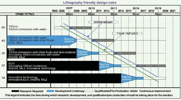
Fig 2: ITRS 2007 Lithography Technology Roadmap (Source: ITRS)
By 2010, the 193nm immersion lithography system has been able to make 32nm process products and play an important role in nodes below 20nm. So the immersion lithography technology has become the most capable and mature technology before EUV.
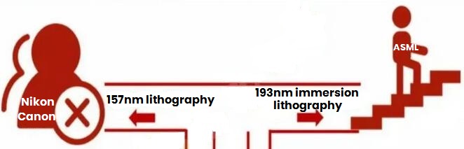
Fig 3: Photolithography Watershed
TSMC has helped ASML a lot in terms of technology, talents, and capital. With TSMC's "immersion lithography" solution, ASML shortened the wavelength of the light source from 193nm to 134nm. Since then, ASML has opened the era of rapid access to the lithography machine market.
EUV Lithography
In order to break through the bottleneck of 193nm lithography, EUV was also one of the directions, but limited by the technical level at that time to realize. From 1997 to 2003, the EUV LLC Alliance had make great effort to promote the research process of EUV lithography technology. Because DUV has been difficult to continue to optimize after the 22nm node. More over, several expected technologies in the 1990s had difficulty to make new progress, the semiconductor industry gradually reached a consensus that extreme ultraviolet (EUV) wavelength lithography technology was a new way. With the time goes by, EUV has become the new technique of chip companies such as Intel, TSMC, and Samsung in recent years. As of 2023, ASML Holding is the only company who produces and sells EUV systems for chip production, targeting 5 nm and 3 nm process nodes.
Since the 157-nm light cannot penetrate pure water, and cannot be combined with immersion technology, therefore, the excimer laser light source has only been developed to ArF. Through immersion lithography and dual lithography, the 4th-gen ArF lithography machine can achieve a maximum process of 22nm for chip production. However, driven by Moore's Law, the demand for chip manufacturing has grown to 14nm and 10nm, even at 7nm, the ArF lithography machine can not make this, so the industry places its hopes on the 5th-gen EUV lithography machine.

Fig 4: EUV Optical System Diagram (Source:Lithography gets extreme)
The most obvious feature of EUV technology is that the exposure wavelength is reduced to 13.5nm, which has more advantages in lithography precision patterns than 193nm DUV. EUV can reduces process steps, improves yield, and can also greatly increase the resolution of the lithography machine. But it also faces challenges, EUV wavelength is too short and the photon energy is very high, basically most materials will absorb EUV light easily, resulting in very weak light intensity when the light source reaches the working surface. So the selection of materials is very critical when designing, and the lithography spacing also requires a strict vacuum environment. In addition, the emergence of a new light source lithography machine must affect the structure of the entire industrial chain, because different light sources have unique requirements for mask materials, photoresist materials, and optical lenses.
From the perspective of manufacturing progress, ASML launched the prototype of the EUV lithography machine in 2006, built a 10,000-square-meter dust-free studio in 2007, and built the first R&D prototype NXE3100 in 2010, and finally had mass production in 2015. During the research and development process, Intel, Samsung, and TSMC have also spent a lot of time and energy on semiconductor manufacturers.
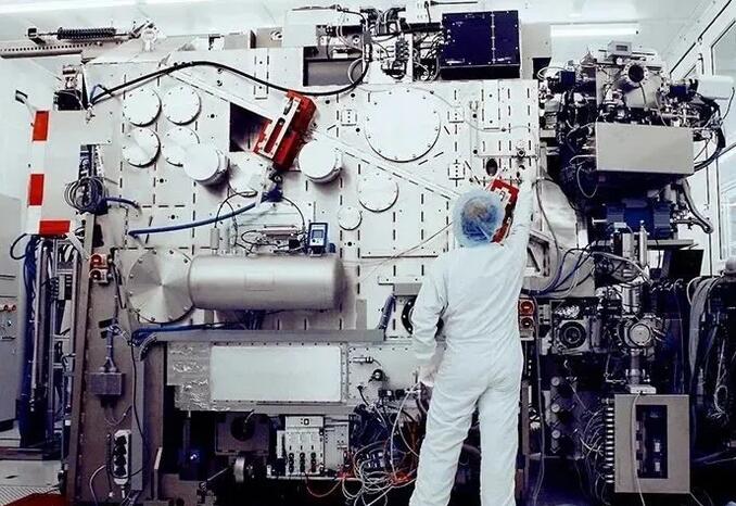
Fig 5: The Prototype of the World's First EUV Lithography Machine In 2006
In 2006, the prototype of the world's first EUV lithography machine.
Since then, ASML has gradually become the unshakable overlord of the lithography machine market with EUV. In 2012, Intel, TSMC, Samsung and other manufacturers invested in ASML to support the improvement and upgrade of EUV lithography technology, and to gain priority supply rights. After 2013, in order to accelerate the development of EUV technology, ASML continued to carry out mergers and acquisitions, such as Cymer, HMI, Mapper, and Berliner Glas, etc. Focusing on EUV, ASML has invested more than 6 billion euros over 20 years, and achieved mass production of EUV machines in 2020. As the only manufacturer sales EUV systems, ASML has naturally received a large number of orders. For example, as of the first quarter of 2022, ASML has shipped 136 EUV systems, and about 70 million wafers have been exposed.
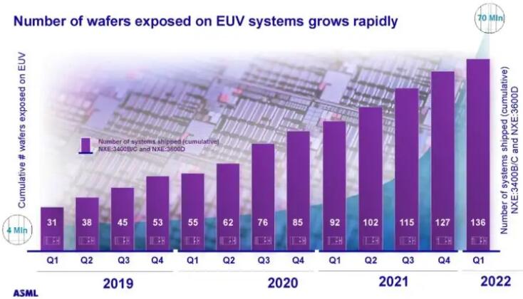
Fig 6: EUV Systems Sales Volume (Source: ASML)
The History of Lithography Machine
According to the improvement of the light source used in the lithography equipment and the process innovation, the lithography machine has experienced 5 generations of product, and each improvement and innovation has significantly improved the minimum process node for chip production.
The 1st gen is a contact proximity lithography machine. The light sources are 436nm g-line and 365nm i-line. This lithography machine contacts with the photoresist directly, so it is easy to get dirty, its reticle and the substrate are easily damaged, and the life of the reticle is short.
The 2nd gen is a proximity lithography machine. The light source is also 436nm g-line and 365nm i-line. The exposure method is that the reticle and the substrate are in a non-close contact state, which reduce the problems of the first generation. However, there is a certain gap between the reticle and the substrate, the imaging quality is affected and the resolution is reduced.
The 3rd gen is a scanning projection lithography machine, which uses optical lenses to gather diffracted light to improve imaging quality. The exposure method is innovated into optical projection lithography, which realizes exposure by scanning. And the light source is also improved to 248nm KrF laser, which realizes the minimum process to 180-130nm.
The 4th gen is a step-and-scan projection lithography machine, the most representative product, first launched by ASML in 1986, using a 193nm ArF laser light source to realize the simultaneous movement of the mask and the silicon wafer, and adopts a reduction projection lens with a ratio of 5:1, which effectively improves the use efficiency and exposure accuracy of the mask, and raises the chip manufacturing process and production efficiency to a new level.
The 5th gen is the EUV lithography machine, which uses a laser plasma light source with a wavelength of 13.5nm. At present, the semiconductor industry's demand for chips has grown to 5nm, or even 3nm, and immersion lithography is facing more challenges of lens aperture and materials. Only EUV lithography machine can advance the minimum process node to 5nm and 3nm now.
Under the current technical conditions, the NA numerical aperture is not easy to increase, and the NA value of the currently used lenses is 0.33. According to ASML, EUV technology will realize a numerical aperture of 0.55. The 0.55 NA EUV machine will continue to enable cost-effective scaling for future nodes, with higher numerical apertures to realize a 1.7x reduction in die size, and further improve resolution. The first EUV 0.55 NA platform early access system is expected to be put into use in 2023, and the customer is expected to start research and development in 2024-2025, and enter the mass production in 2025-2026.
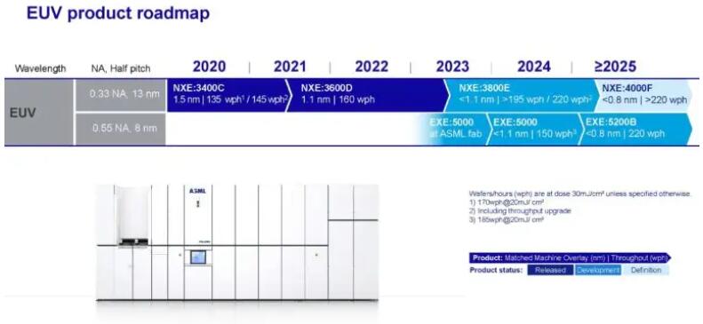
Fig 7: EUV System Roadmap(Source:ASML)
Conclusion
After the completion of the first 0.55 NA lithography equipment, more innovations in lithography tools, masks, and resists are expected to further reduce the K1 factor and allow shrinkage to continue for the next decade.
Throughout the development of lithography technology, this most sophisticated, difficult and expensive technology has continuously promoted the evolution of Moore's Law in the long time, allowing the global semiconductor industry to follow suit. However, high R&D costs and difficulties have brought lithography technology to a fork in the road again and again. At the same time, under the impetus of Moore's Law and the market, lithography technology also has ushered in breakthroughs again and again.
Anyone interested in semiconductor industry, just visit KUKE Electronics to learn more.